
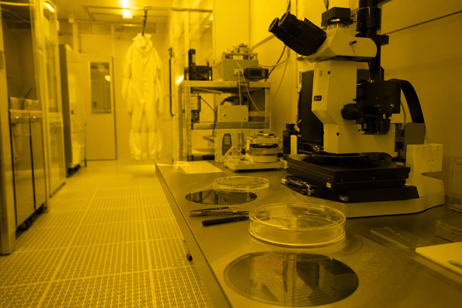
Used for III-V and silicon photonic process development. Industrial partners typically come for process lots, failure analysis, or a student who already knows the tool.
Work packages should specify wafers, process steps, and who owns the IP in words a lawyer will not later enjoy.
The intellectual property point is not a formality. Process development in a shared cleanroom generates knowledge that is difficult to partition: a recipe improvement discovered during your lot may be indistinguishable from general process knowledge. Settling in advance what is background, what is foreground and what may be published prevents a genuinely awkward conversation later.
Users should also plan for packaging. Fibre attachment, thermal management and hermetic sealing are where photonics programmes most often stop, and a facility that produces a working die but no route to a packaged device has solved the interesting half of the problem and not the commercial one.
Specification
- Class 100 / 1000 bays
- Lithography and etch
- On-wafer optical test
- Deposition and metallisation
- Dicing, cleaving and facet preparation
- Characterisation of loss, coupling and spectral response
What it is the right answer to
Jobs this facility genuinely suits.
- Process development for a new waveguide or detector design
- Shared process lots where several parties need the same development
- Failure analysis on devices that underperform against simulation
- Small-volume fabrication for prototypes and qualification samples
- Training an engineer on tools they will later use in a foundry
What to bring
Turning up without these costs facility hours rather than bench hours.
- A mask set or a design mature enough to commit to one
- Wafers, or a decision to use the facility's stock and its consequences
- A written position on background and foreground intellectual property
- A plan for packaging and test, ideally in the same work package
What you leave with
- Processed wafers or die with a full process record
- On-wafer optical characterisation data
- Process notes sufficient to attempt a transfer to a foundry
- Yield data, which is frequently the most valuable output
Limitations
Worth knowing before you write the proposal.
- Research cleanroom yields are not foundry yields and should not be quoted as such
- Process transfer to a commercial foundry is a separate and substantial exercise
- Volume production is not available here and never will be